
DRAM research is difficult. Work that aims to be applicable to commodity devices should consider the sense amplifier internal layouts, transistor dimensions and circuit typologies used by real devices. These are all essential elements that must be considered while proposing new ideas. Unfortunately, they are not disclosed by DRAM vendors. As such, researchers are forced to make assumptions about these important aspects, impacting the accuracy of their proposals.
To overcome these challenges, we performed IC imaging of 3 DDR4 and 3 DDR5 chips from the three major DRAM vendors as shown in the video above. Then, we reverse engineered the sense amplifier region, and measured relevant dimensions (e.g., transistor widths). With the acquired information, we looked at the accuracy of DRAM research in the past 10 years. We made multiple discoveries (please read the paper!), summarized as:
Topology (1) : In half of the chips, the commonly assumed classical sense amplifier is replaced by the offset-compensating topology. This was never reported before in literature, and no prior work considered this topology to be used.
Dimensions (2): Analog DRAM models are optimistic about the transistor dimensions. In the worst case, the inaccuracy is up to 9x.
Research inaccuracies (3): We identify multiple research inaccuracies that are shared across different papers in a range of 10 years. For example, a common aspect is assuming that there is space for connections in the bitline metal layer.
Overhead inaccuracies (4): Once the research inaccuracies are accounted for in the calculations for the area overhead, many papers are subjected to a much larger overhead than originally estimated in the paper.
We hope that HiFi-DRAM will increase the fidelity of future DRAM research. We conclude the paper by providing a list of recommendations for future research.
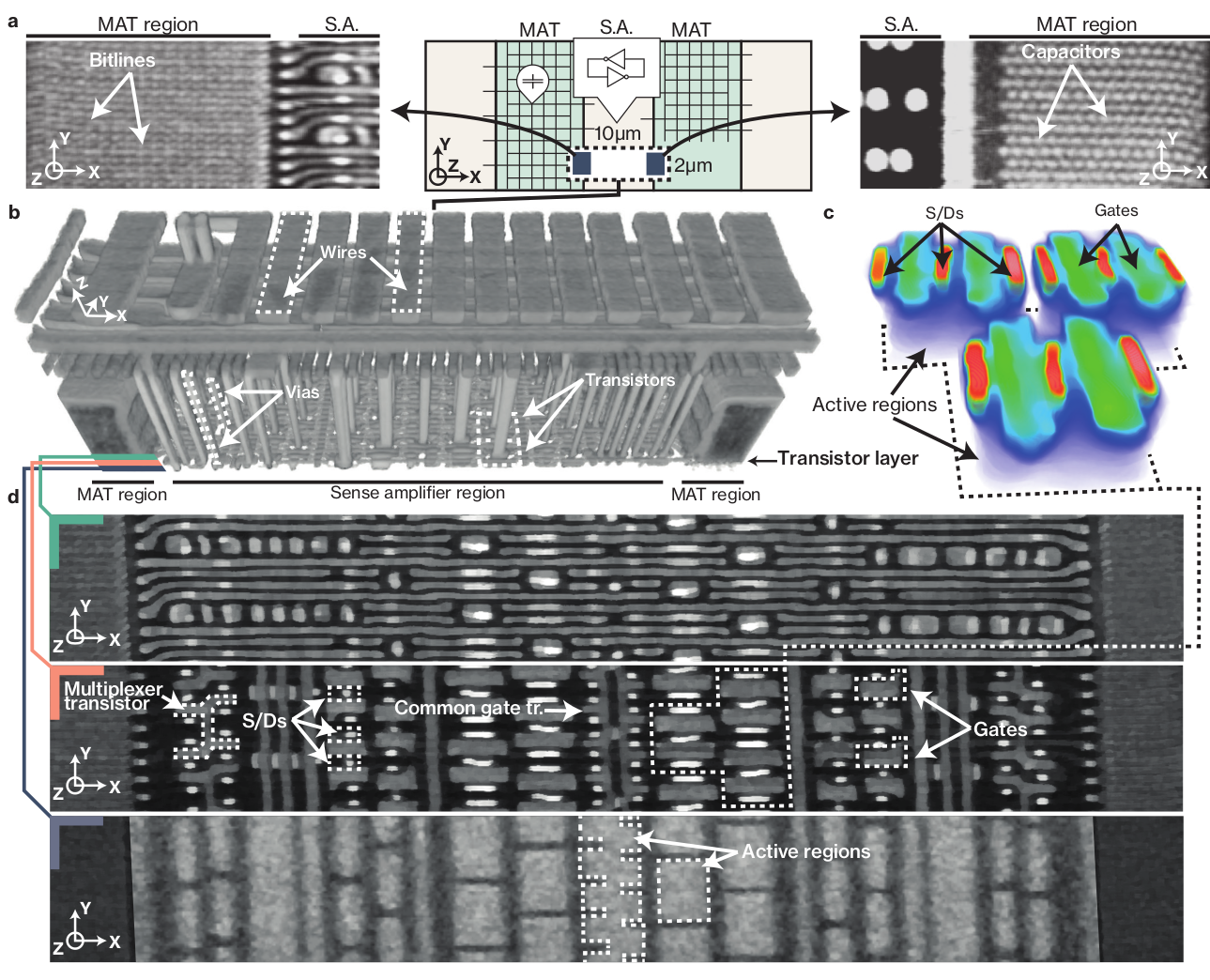
Fig. 1: You can the 3D reconstruction of a sense amplifier region. For more details about these images please refer to the paper.
What are sense amplifiers?
DRAM memory is based on capacitors storing data as charge. When memory is accessed, the sense amplifiers have the task of sensing, and then amplifying, this extremely weak signal.
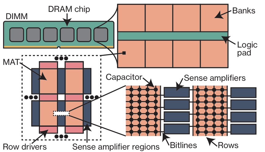
Fig. 2: A DIMM contains several DRAM chips, each made of multiple banks. A bank has many MATs, filled with capacitors. Capacitors are connected to SAs via bitlines after they are selected by rows. SAs are in between MATs.
Sense amplifiers impact the speed of data communication with DRAM. Some research, for example, modifies this region to reduce the delay required to access data. At the same time, sense amplifiers have access to large amounts of data (e.g., 8KB). Research exploits this parallelism to perform Processing-In-Memory (PIM). Finally, because of Rowhammer, this region can be modified to accommodate new mitigations (such as our REGA).
How did you image sense amplifiers?
We performed Scanning Electron Microscopy (SEM) with the aid of Focused Ion Beam (FIB). SEM allows us to image at a very low scale (i.e., not optically visible). Instead, FIB can cut away material to allow us to image the different integrated circuit (IC) layers. Please, read the paper for more details.

Fig. 4: FIB/SEM imaging requires an ion beam and an electron gun, under which the sample is positioned. The BSE detector is placed on the electron gun, while the SE detector is skewed. FIB/SEM allows to image the cross section of an IC. An IC is made of multiple metal layers, which are interconnected by vias. The transistor layer is placed at the bottom of the IC.
What did you do with the acquired data?
We evaluated existing DRAM analogue models in terms of transistor widths and lengths. Then, we studied existing literature to understand common wrong assumptions shared by researchers. We classified 5 different inaccuracies (I1-I5). Finally, we evaluated the overhead errors of past research, given commodity DRAM devices.
Based on our findings, we provide 4 recommendations that we hope future research will follow.
In general, we discovered that relying on dual-contact cells (DCC) leads to severe area overheads, never considered in the original papers employing them.
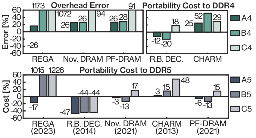
Fig. 5: Research portability cost and overhead error divided per DRAM vendor. Papers where the cost/error is always higher than 10x are omitted.
What are the recommendations for future research?
Our recommendations for future work are as follows:
- Overheads should be estimated including all additions to MATs or sense amplifiers, such as wire connections.
- Research modifying sense amplifiers should consider the impact on all the interconnected sense amplifiers.
- Research should consider the physical layout and organization of sense amplifiers blocks.
- Research should consider offset-compensating sense amplifiers in their evaluation.
More information
Our paper, HiFi-DRAM, is available now and will officially be presented at ISCA 2024. You can find all the extracted data on GitHub.
FAQs
Following, we provide answers to the most frequently asked questions about our work.
- How do you envision Hi-Fi DRAM helping DRAM research?
Hi-Fi DRAM gives researchers the information to correctly estimate overheads, as well as layouts of their research. These important details have so far been approximated, with many assumptions throughout the years.
- Is this approach applicable to other memory technologies as well?
Yes, our approach is applicable to different memory technologies (e.g., GDDR) as well.
- You report high overheads for some research. How does this impact previous research value?
We do not believe this aspect to remove value from these papers. Early papers have discussed novel ideals and generated a high sprout of subsequent works. Please refer to “On existing and future work.” in our paper.
- Do you plan to open-source the extracted data?
Yes! You can find it on GitHub.
Acknowledgments
This work was supported by the Swiss National Science Foundation under NCCR Automation, grant agreement 51NF40 180545, the Swiss State Secretariat for Education, Research and Innovation under contract number MB22.00057 (ERC-StG PROMISE), and a Microsoft Swiss JRC grant.